
Semiconductor manufacturing is one of the most advanced industries in the world and requires extreme accuracy and strict quality control. Even the tiniest contamination can reduce sales of chips making them uncompetitive.
This has been a fervent effort for manufacturers like IBM. They’ve turned Inductive Coupling Mass Analysis (ICP-MS) into an analytical machine of peerless sensitivity, maintaining its ground on par with the best in chip-making automation. That is why ICP-MS plays an essential role in semiconductor manufacturing today, by ensuring that companies can achieve precision standards and regulations set down for the industry.
What Is ICP-MS and Why It Matters
ICP-MS for Semiconductor Manufacturing Automation & Compliance is an analytical technique that takes advantage of plasma to ionize samples and a mass spectrometer to measure trace elements in parts-per-billion concentrations. It is crucial for such a capability to exist in semiconductor manufacturing because our modern devices demand near perfection in their materials. To detect contaminants at parts per trillion levels ensures that wafers, chemicals and gasses all meet the demanding purity standards of our industry.
Without ICP-MS, it would nearly be impossible to reach the present accuracy demanded for microchips, the machinery behind everything from cellular phones to medical equipment.
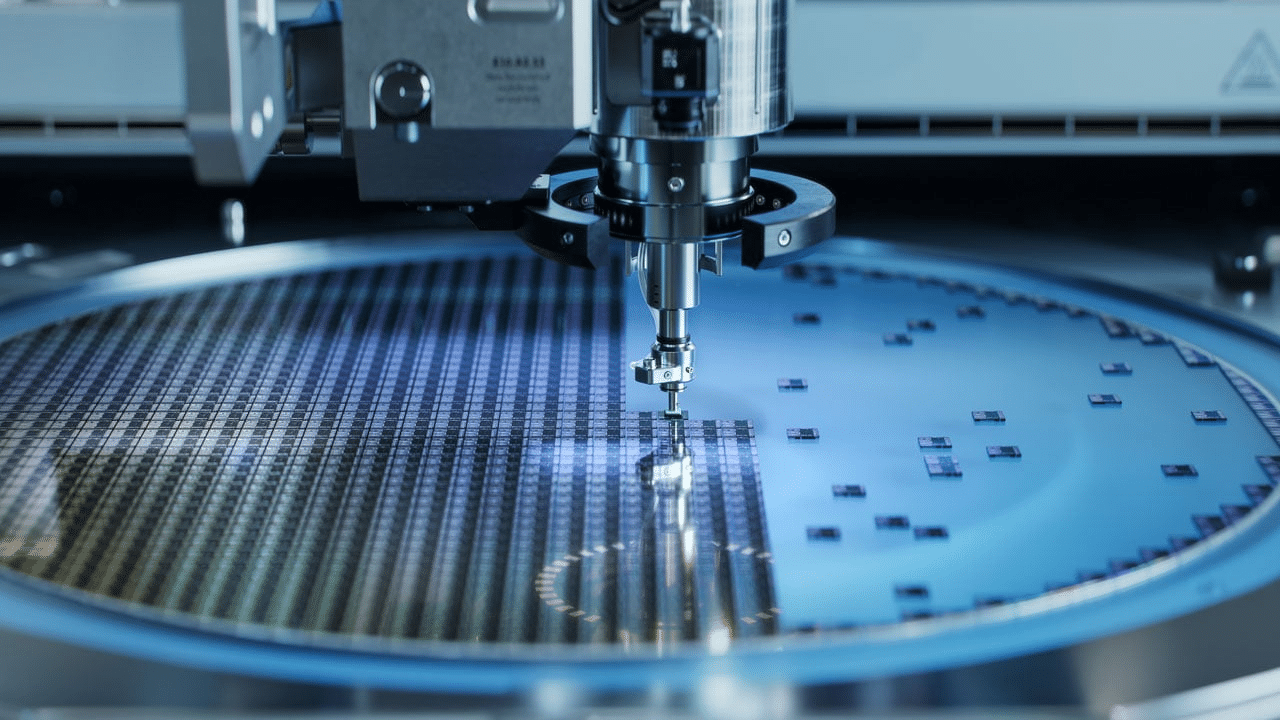
The Role of Automation in Semiconductor Manufacturing
To raise productivity and quash human errors, conveying manufacturers heavily on automation. It operates systems that handle chemicals, process wafers, and inspect quality. Automating workflows with ICP-MS makes impurity testing fast, repeatable, and consistent across whole runs of production.
Because of this synergy between automation and ICP-MS there is less time wasted between jobs–and therefore more products come out in a given year for the same facility costs as before.
Compliance with Industry Standards
The semiconductor industry is trying to adhere to standards from around the world, including those of SEMI (Semiconductor Equipment and Materials International). One type of such standards even sets the purity of materials, limitations on contamination, and safety regimes.
With ICP-MS compliance, manufacturers can ascertain both the purity of their raw materials as well as if they’ve met international standards in processing them. Not only is this necessary to preserve product reliability but also means that firms can take part in the global market, where to conduct commercial transactions compliance is often a necessary precondition.
Applications of ICP-MS in Semiconductor Manufacturing
ICP-MS is applied at many different points in the semiconductor supply chain, including:
Evaluation of raw materials: nobody silicon, gases, and chemicals.
Process monitoring: review the contamination in etching, deposition, and cleaning.
Waste management: regulates pollution discharge in order to meet standards.
Final product quality control: These checks ensure wafers or apparatus substring components devices on them in a clean environment with no trace contaminants
Functions like these get the work done with you can’t even remember how and so in terms of effectometers ICp-MS operator finds their use vital to semiconductor manufacturing efficiency and control of raw material quality.
Benefits of ICP-MS in Manufacturing
Some benefits in semiconductor manufacturer installations for ICP-MS are:
Unrivaled sensitivity: It detects impurities at extremely low concentrations.
Speed and efficiency: automation ensures that tests take less time
Consistency-hence control over quality: Reliable test results give stable product quality
Regulatory compliance: It is in line with the world’s stringent quality standards
Lowers Risk: prevents product recalls because of contamination, thereby saving massive costs.
ICP-MS is one of the most valuable tools available to fabs that want both the utmost in quality and high productivity.
Challenges and Solutions
A major challenge in using inductively coupled plasma mass spectroscopy, or ICP-MS, lies in the need for complex sample preparation procedures and maintenance. As with this both of the whole system has to come to a standstill, until the problem is solved.
Automation remedies both problems: by standardizing processes it reduces mistakes; through all times monitoring it allows inspecting of things without stopping their manufacture (which might be a great deal more important for semiconductor plant human factors reasons).
Also, modern ICP-MS systems are produced in general with input from the semiconductor device manufacturer to facilitate maximum convenience in utilization.
Future Outlook
With smaller chips, faster chips and computers that are more powerful, the need for precision manufacturing of semiconductors will only be more pressing. Supported by advances in automation and data analytics, ICP-MS will remain as the central technology.
In the future, factories may incorporate real-time monitoring with prediction ability so that any potential problems can be anticipated before they actually happen on the line. This will bring still closer together ICP-MS–automation–and compliance.
Precision Meets Compliance
In semiconductor manufacturing, which is a highly competitive field, no mistakes will be tolerated. ICP-MS technology for semiconductor manufacturing automation and compliance ensures that every aspect of the production process complies with the highest standards. From minute particles of pollutants to global compliance, ICP-MS is the key to today’s reliable technologies.
By adding automation to sensitive detection, manufacturers gain a powerful tool that is both productive and reliable. ICP-MS will continue to be foundational for precision and compliance as semiconductor technology advances further and further.